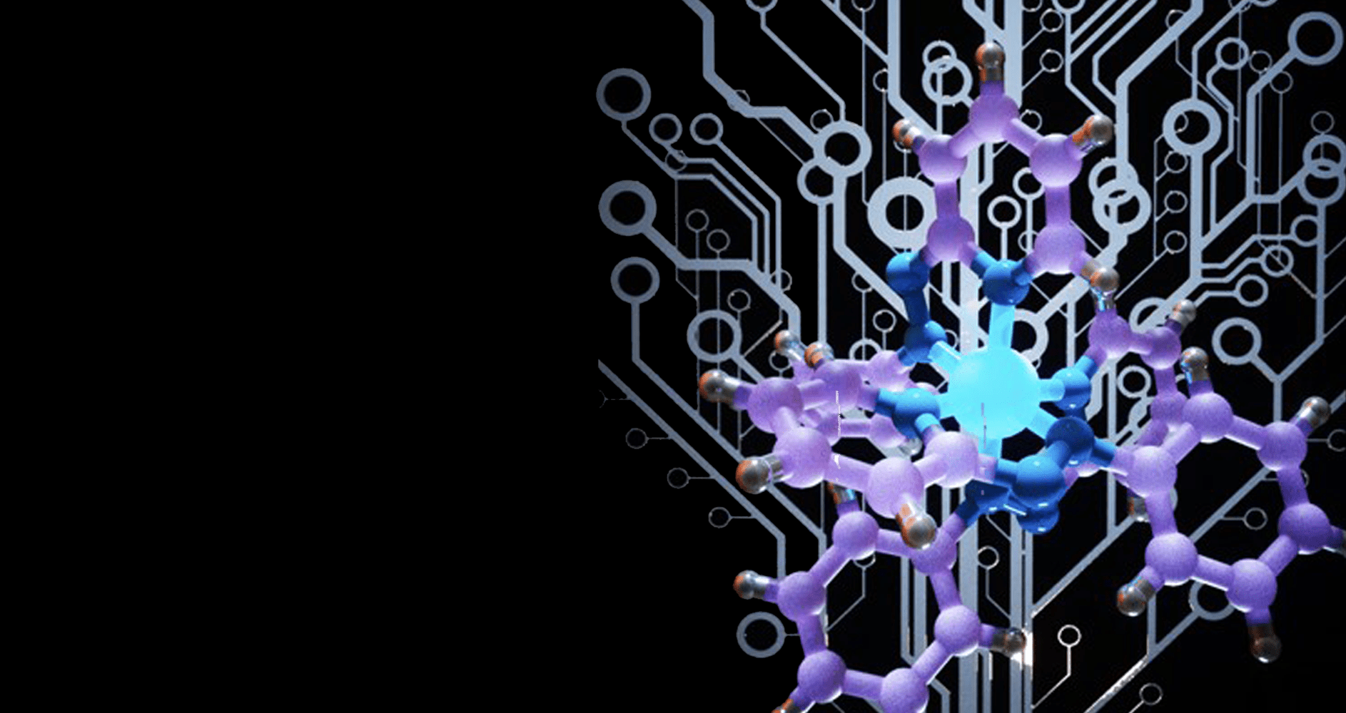
NUS researchers develop brain-inspired memory device that can revolutionise semiconductor design
Reconfigurable device can simplify semiconductor circuit design and enhance computational power and speed
Many electronic devices today are dependent on semiconductor logic circuits based on switches hard-wired to perform predefined logic functions. Physicists from the National University of Singapore (NUS), together with an international team of researchers, have developed a novel molecular memristor, or an electronic memory device, that has exceptional memory reconfigurability.
Unlike hard-wired standard circuits, the molecular device can be reconfigured using voltage to embed different computational tasks. The energy-efficient new technology, which is capable of enhanced computational power and speed, can potentially be used in edge computing, as well as handheld devices and applications with limited power resource.
“This work is a significant breakthrough in our quest to design low-energy computing. The idea of using multiple switching in a single element draws inspiration from how the brain works and fundamentally reimagines the design strategy of a logic circuit,” said Associate Professor Ariando from the NUS Department of Physics who led the research.
The research was first published in the journal Nature on 1 September 2021, and carried out in collaboration with the Indian Association for the Cultivation of Science, Hewlett Packard Enterprise, the University of Limerick, the University of Oklahoma, and Texas A&M University.
Brain-inspired technology
“This new discovery can contribute to developments in edge computing as a sophisticated in-memory computing approach to overcome the von Neumann bottleneck, a delay in computational processing seen in many digital technologies due to the physical separation of memory storage from a device’s processor,” said Assoc Prof Ariando. The new molecular device also has the potential to contribute to designing next generation processing chips with enhanced computational power and speed.
“Similar to the flexibility and adaptability of connections in the human brain, our memory device can be reconfigured on the fly for different computational tasks by simply changing applied voltages. Furthermore, like how nerve cells can store memories, the same device can also retain information for future retrieval and processing,” said first author Dr Sreetosh Goswami, Research Fellow from the Department of Physics at NUS.
Research team member Dr Sreebrata Goswami, who was a Senior Research Scientist at NUS and previously Professor at the Indian Association for the Cultivation of Science, conceptualised and designed a molecular system belonging to the chemical family of phenyl azo pyridines that have a central metal atom bound to organic molecules called ligands. “These molecules are like electron sponges that can offer as many as six electron transfers resulting in five different molecular states. The interconnectivity between these states is the key behind the device’s reconfigurability,” explained Dr Sreebrata Goswami.
Dr Sreetosh Goswami created a tiny electrical circuit consisting a 40-nanometer layer of molecular film sandwiched between a top layer of gold, and a bottom layer of gold-infused nanodisc and indium tin oxide. He observed an unprecedented current-voltage profile upon applying a negative voltage to the device. Unlike conventional metal-oxide memristors that are switched on and off at only one fixed voltage, these organic molecular devices could switch between on-off states at several discrete sequential voltages.
Using an imaging technique called Raman spectroscopy, spectral signatures in the vibrational motion of the organic molecule were observed to explain the multiple transitions. Dr Sreebrata Goswami explained, “Sweeping the negative voltage triggered the ligands on the molecule to undergo a series of reduction, or electron-gaining which caused the molecule to transition between off and on states.”
The researchers described the behavior of the molecules using a decision tree algorithm with “if-then-else” statements, which is used in the coding of several computer programs, particularly digital games, as compared to the conventional approach of using basic physics-based equations.
New possibilities for energy-efficient devices
Building on their research, the team used the molecular memory devices to run programs for different real-world computational tasks. As a proof of concept, the team demonstrated that their technology could perform complex computations in a single step, and could be reprogrammed to perform another task in the next instant. An individual molecular memory device could perform the same computational functions as thousands of transistors, making the technology a more powerful and energy-efficient memory option.
“The technology might first be used in handheld devices, like cell phones and sensors, and other applications where power is limited,” added Assoc Prof Ariando.
The team in the midst of building new electronic devices incorporating their innovation, and working with collaborators to conduct simulation and benchmarking relating to existing technologies.
Other contributors to the research paper include Abhijeet Patra and Santi Prasad Rath from NUS, Rajib Pramanick from the Indian Association for the Cultivation of Science, Martin Foltin from Hewlett Packard Enterprise, Damien Thompson from the University of Limerick, T. Venkatesan from the University of Oklahoma, and R. Stanley Williams from Texas A&M University.
Press Release:
NUS Research News, 2 September 2021
Coverage:
NUS Spokesperson Twitter, 2 September 2021
(copy https://twitter.com/NUSspokesperson/status/1433284285000138752 into web browser)
NUS Twitter, 3 September 2021
(copy https://twitter.com/NUSingapore/status/1433602420886499347 into web browser)
NUS Research Twitter, 3 September 2021
(copy https://twitter.com/NUSResearch/status/1433602647341207552 into web browser)
NUS Facebook, 3 September 2021
NUS LinkedIn, 3 September 2021
ZDNet, 2 September 2021
Singapore researchers develop ‘reconfigurable’ memory chip technology
Computer Weekly, 2 September 2021
NUS researchers develop brain-inspired memory device
Science Daily, 2 September 2021
Brain-inspired memory device
Mirage News, 2 September 2021
Researchers develop brain-inspired memory device that can revolutionise semiconductor design
Techiai.com, 3 September 2021